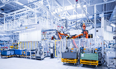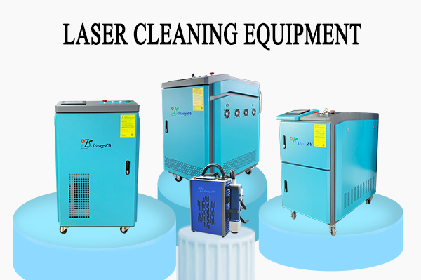
Laser cleaning is a new type of green and environmentally friendly cleaning method. The pulsed laser used has a long service life and is suitable for hand-held and robot cleaning operations. It has a universal wheel and is easy to move.
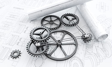
At present, with the continuous miniaturization of semiconductor technology, advanced integrated circuit devices have been transformed from planar to three-dimensional structures, and the integrated circuit manufacturing process is becoming more and more complex, often requiring hundreds or even thousands of process steps. For advanced semiconductor device manufacturing, there will be more or less particle contaminants, metal residues or organic residues on the surface of the silicon wafer after each process. The shrinking feature size of the device and the increasing complexity of the three-dimensional device structure make semiconductor devices more and more sensitive to particle contamination, impurity concentration and quantity.
The cleaning technology of contaminating particles on the surface of the mask on the silicon crystal element has put forward higher requirements. The key point is to overcome the great adsorption force between the contaminating microparticles and the substrate. At present, many semiconductor manufacturers clean by pickling and manual wiping, which is not to mention slow efficiency, but also produces secondary pollution. So what kind of cleaning method is more suitable for cleaning semiconductor products? Laser cleaning is a more suitable way at present. When the laser scans, the dirt on the surface of the material is removed, and the dirt in the gaps can be easily removed, without scratching the surface of the material or causing secondary pollution. It is a safe choice.
In addition, as the size of integrated circuit devices continues to shrink, material loss and surface roughness during the cleaning process become issues that must be paid attention to. Removing particles without material loss and pattern damage is the most basic requirement. Laser cleaning technology has the advantages of non-contact, no thermal effect, no surface damage to the object to be cleaned, and no secondary pollution. It is the best cleaning method to solve the pollution of semiconductor devices.

Win the market with technological leadership and reward users with high-quality services
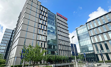
Shengtong Intelligent Machinery Equipment (Shanghai) Co., Ltd.
Shanghai Shengtong Laser Equipment (Group) Co., Ltd.
Shengtong Intelligent Laser Equipment (Dalian) Co., Ltd.
Xi'an Shenghong Laser Intelligent Equipment Co., Ltd.
Shanghai Chengjing Industrial Development Co., Ltd.
Zhizhuo (Shanghai) Technology Co., Ltd.
Contact Person��Manager Xu
Phone��021-54850067
E-mail��rongqing@shengtongzn.com
Address: Building 12, No. 6055, Jinhai Road, Fengxian District, Shanghai